
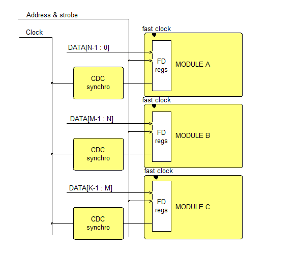
A few months ago I have came across an interesting implementation problem. Xilinx Vivado IDE has a curious optimization strategy. This occurs in a situation where each module of a design is in a different CDC (clock domain cross) zone. Sample diagram of such HDL design is here:
After Xilinx Vivado IDE synthesis everything was well connected. Situation was a little different after place and route process. Xilinx Vivado implemenation process did some magic. I suppose that for better timing closure in UltrascalePlus devices Vivado tool shares some nets between modules. Those nets are denoted as “alias” nets.
In my case the FD latch regs enables lines was activated by neighbors modules. It can be seen below where left module (different CDC zone) drives right module flip flops.
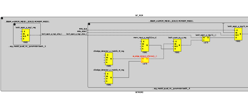
From the pure logic point of view its correct, but if you take metastability phenomena into consideration situation looks a lite different. Flip flops inside a single module can be activated at different cycle of fast clock.
It has made a few weeks of deep dive debugging in a hardware.